.png)


Printed photovoltaics: challenges and issues


This technology, still in development, combines cost, flexibility, and environmental benefits, with laboratory yields nearly on par with existing methods. But what makes these cells so special, and what challenges remain to be overcome for their widespread adoption?
- The Challenges of Manufacturing a Solar Cell
Current methods for manufacturing photovoltaic cells involve stacking different layers of materials that make up the electrodes, the charge carriers, and the semiconductor that reacts to light, as well as additional layers to stabilize the assembly.
Each of these layers must be both chemically and physically compatible with the adjacent layers. Some must also possess specific optical properties; the surface electrode must be transparent, which, in scientific terms, is referred to as transmittance—that is, a material’s ability to allow light to pass through. Ideally, this should be 100%, but in practice, for the surface electrodes of current solar cells, it is around 85%. Only graphene, as a conductive material, has a transmittance greater than 90%. See the challenge? Now let’s add a cost constraint so that the technology can actually leave the lab: an average cost per square meter of less than €100, or about 30 cents per watt produced.
It is on these aspects that GRAPHENATON Technologies SA (GTSA), through its GRAPHENATON Labs, is conducting its research programs to develop a solar cell that is sufficiently efficient yet environmentally responsible while remaining economically viable.
The challenges identified concern all layers, and more specifically the electrodes and the semiconductor material. Regarding the former, GTSA is working on the use of graphene in particular; regarding the latter, GTSA has launched a research program on perovskites.
The R&D teams also faced two key challenges: first, working in ambient conditions to ensure that future industrial applications would be cost-effective; and second, printing the entire cell in a single process to facilitate large-scale production and, as a result, identify the most suitable inks and substrates.
- Tin perovskites: a promising alternative to lead perovskites
Perovskites, particularly lead-based ones, have attracted the attention of researchers due to their remarkable efficiency and laboratory performance close to that of silicon (27.6% efficiency for silicon versus 26.1% for perovskites) [1]. However, the toxicity of lead poses long-term environmental and health concerns. GTSA offers a less toxic alternative: tin perovskites.
Tin perovskite-based solar cells utilize a well-known metal halide perovskite structure, but with tin—which is far less toxic—replacing the traditionally used lead [2]. This active layer exhibits properties conducive to converting light into electricity with a lower environmental impact. It can also be produced using an “ink” and can be customized to suit different materials [3][4][5]. The first prototypes produced confirm their technical feasibility using low-cost materials.
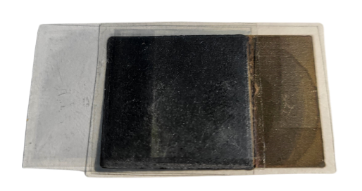

Figure 1: GTSA prototype of a 2 cm x 2 cm printed tin-perovskite solar cell (left) -
Current response of the cell prototype under light and in the dark (right)
- Innovative printing techniques …
What truly sets the perovskite-based solar cells designed by GTSA apart is their manufacturing method. Unlike traditional solar cells, these cells can be printed onto flexible polymer substrates.
This process is used to develop “functional inks” containing all the precursors—essentially the building blocks—that will form the perovskite. Once deposited via printing, the various components self-assemble to form a thin crystalline structure capable of reacting to light.
Printing techniques such as inkjet allow these thin layers to be deposited with precision and efficiency. They are also less expensive than conventional methods; only the necessary amount of ink is used, and annealing processes are carried out at much lower temperatures than conventional methods—120°C or less, compared to over 1,000°C for silicon purification. This avoids costly waste treatment processes, minimizes excess energy consumption during manufacturing, and eliminates the need for highly restricted production environments in cleanrooms.
These printing technologies would also make it possible to produce films that break away from the standard panel sizes (1.65 m²/60 cells, 2 m²/70 cells) for new applications.
4 … Challenges waiting to be tackled
However, there are still many challenges to overcome.
First, regarding the active layer itself. Perovskites, particularly tin-based ones, are more sensitive to moisture and oxygen—whether during the manufacturing process or over the long term during use—which can lead to a rapid decline in performance. Research efforts are underway to develop new functional inks that are fully compatible and highly stable for printing in a standard environment—areas in which GTSA is actively engaged.
Furthermore, to be fully functional and capture as much light as possible, the layers between the photosensitive layer and the surface must be not only conductive but also transparent. The materials of choice for transparent surface electrodes are currently ITO (indium tin oxide) layers, which rely on rare earth elements. In addition to the lack of flexibility in these layers, the use of these rare earth elements poses sovereignty issues (90% of reserves are held by China, Vietnam, Brazil, and Russia; specifically for indium, China alone produces two-thirds of global consumption [6][7]). This is why GTSA wishes to turn to graphene electrodes. Composed of carbon atoms arranged in a hexagonal lattice, this material—whose transparency and conductivity equal or surpass those of ITO—is a perfect candidate. In the proposed application, a polymer film is used on which a thin sheet of graphene has been grown under vacuum in a controlled manner, which is subsequently used as a printing substrate. However, the main challenge lies in its economic viability, since its current price is around €5,000/m². This is why, for surface electrodes, GTSA is also exploring the possibility of using polymers incorporating carbon nanotubes or metal nanowires. But graphene can also be used in the form of an ink. In this form, it is opaque but can still be used as a back electrode (the electrode located at the back of the cell), where certain properties—such as its excellent conductivity—are leveraged.
- Outlook
Stainless perovskite-based solar cells printed under ambient conditions represent a significant breakthrough in the field of photovoltaic cells by eliminating the use of lead. Their potential to offer a less toxic, flexible, and cost-effective alternative has been proven.
GTSA has launched research programs through its R&D subsidiary, GRAPHENATON Labs, based at Paris Cité University. To date, while these programs have validated the scientific hypotheses under consideration, they have not yet delivered energy performance capable of competing with existing solutions. A few laboratories around the world are working on similar issues, and progress is being made rapidly.
GTSA believes it should be able to produce printed photovoltaic cells on a pre-industrial scale by 2025, while taking economic constraints into account.
The commercial applications of these thin-film photovoltaic cells are vast and could revolutionize large-scale photovoltaic power generation.